About JCPCB
18 years of PCB manufacturing excellence. Our 50,000m² facility in Shenzhen, China produces circuit boards for clients in 86+ countries worldwide.
Who We Are
JCPCB was founded in 2008 in Shenzhen, China — the heart of global electronics manufacturing. What began as a focused PCB workshop has grown into a 50,000m² state-of-the-art production campus with 600+ employees serving clients in 86+ countries.
We are not a trading company or a broker. We own and operate our production lines — from copper-clad laminate to finished, tested boards. This vertical integration means we control every step of the process, delivering consistently better quality, faster turnaround, and pricing that trading companies simply cannot match.
Our client list spans Fortune 500 companies, Y Combinator startups, defense contractors, and medical device manufacturers. We hold ISO 9001:2015, ISO 14001:2015, IATF 16949, and UL certifications. Every board is backed by our zero-defect guarantee.

The JCPCB Advantage
Why companies around the world choose to work with us
Own Production Facility — Not a Trading Company
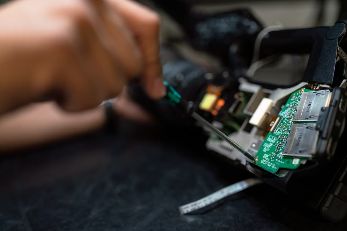
We operate our own 50,000m² manufacturing campus in Shenzhen with 600+ employees and 80+ engineers. No subcontractors. No middlemen. When you talk to our team, you're talking directly to the people who make your boards.
80+ Engineers — Free DFM Service
Every single design file is reviewed by our engineering team before production begins. We catch an average of 3 issues per design that would have caused costly re-spins. This service is completely free — and it has saved our clients over $15,000 per project on average.
Zero-Defect Guarantee
100% electrical testing + AOI + X-ray inspection on every board. IPC Class 3 capable. If any board fails your incoming inspection, we reprint and ship the entire batch for free — no questions asked, no arguments.
Dedicated English-Speaking Account Manager
No ticket queues, no chatbots. You get a named account manager who knows your project, responds within 30 minutes during business hours, and handles everything from quote to delivery. Full English communication.
Industries We Serve
PCB solutions across a wide range of applications
Trusted by leading companies worldwide
Our Journey
18 years of growth alongside the global electronics industry
Founded in Shenzhen — started with single-sided and double-sided PCB production lines
Expanded to multilayer production (up to 12 layers), achieved ISO 9001 certification
Launched HDI production line with laser drilling capability. Signed first Fortune 500 client
Added flexible PCB (FPC) and rigid-flex manufacturing capabilities
Began full turnkey PCBA services. Achieved IATF 16949 automotive certification
Production capacity exceeded 50,000m²/month. Client base grew past 1,000 active accounts
Served customers in 60+ countries. Named Top 10 PCB supplier in Southern China
Opened high-frequency PCB division (Rogers/PTFE hybrid stackups). Passed UL certification
Exceeded 15,000 projects delivered. Expanded international reach to 80+ countries
Now serving 86+ countries with 99.4% on-time delivery rate. 4,200+ active clients
World-Class Equipment
We reinvest 30% of revenue into new equipment — all machines under 3 years old
Orbotech Paragon LDI
Laser Direct Imaging — 1.5/1.5mil line/space. No film, no alignment errors. 4 units installed post-2022.
Hitachi Via Mechanics
High-speed mechanical drilling — 0.10mm minimum. 200+ hits/second. Spindle accuracy ±5μm.
Mitsubishi CO₂ Laser
Micro-via drilling — 0.075mm minimum diameter. For HDI any-layer via formation.
Dima Excellence Plating
Vertical continuous plating lines. Copper thickness uniformity ±2μm across panel.
Koh Young Zenith AOI
3D automated optical inspection — 100% board coverage. 15μm defect detection.
Nordson DAGE XD7800
X-ray inspection system — BGA/QFN voiding analysis. 0.1μm feature resolution.
Our Quality Commitment
Every board is inspected and tested before it leaves our facility
Free DFM Engineering Review
Our 80+ engineers review EVERY design before production — for free. We catch an average of 3 issues per design that would have caused costly re-spins. This alone saves our clients $15,000+ per project.
100% Electrical Testing
Every single board — no exceptions — undergoes flying probe or fixture-based electrical testing. We also perform AOI, X-ray (for BGA/QFN), and visual inspection. Zero boards ship untested.
Zero-Defect Guarantee
If ANY board fails your incoming inspection, we reprint the entire batch for free and ship it via DHL express at our expense. No arguments, no delays, no fine print.
Full Material Traceability
Every production lot ships with material certificates (COA), production records, test reports, and a Certificate of Conformance signed by our Quality Director. Full traceability for 5+ years.
Certifications
ISO 9001:2015, ISO 14001:2015, IATF 16949 (automotive), UL 94V-0. We audit our own processes quarterly — stricter than most certification bodies require.
Dedicated QA Team
40+ full-time quality inspectors across 3 shifts (24/7 production, 24/7 inspection). Our QA team is independent from production — they report directly to the CEO.
Ready to Work With Us?
Whether you need a quick prototype or ongoing production, our factory is ready.